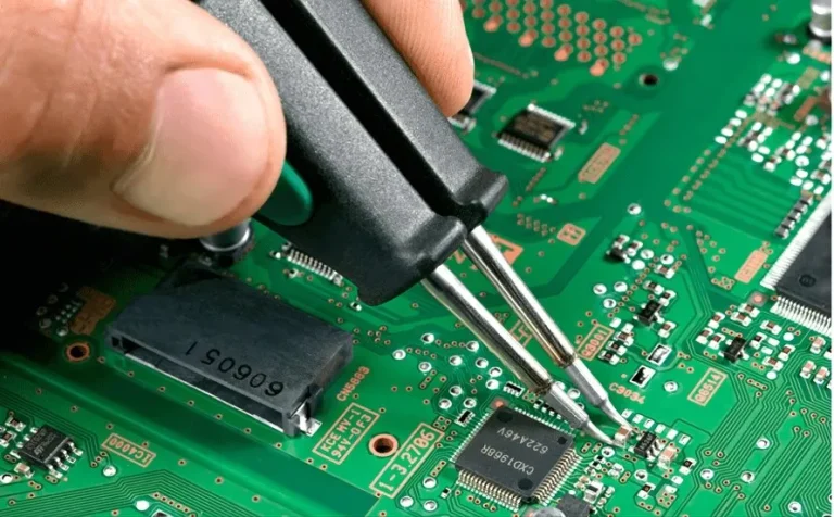
Surface Mount Technology (SMT) has revolutionized the electronics manufacturing industry by enabling the production of smaller, lighter, and more complex electronic devices. However, despite its many advantages, SMT is not without its challenges. Understanding the common defects that can occur during the SMT process is crucial for maintaining high-quality standards and minimizing production costs. This article provides a comprehensive SMT defect list, detailing common issues and their solutions.
1. Introduction to SMT Defects
Surface Mount Technology involves mounting electronic components directly onto the surface of printed circuit boards (PCBs). While this method offers numerous benefits, including improved performance and miniaturization, it also introduces potential defects that can affect the functionality and reliability of the final product. Identifying and addressing these defects early in the manufacturing process is essential to ensure the quality and longevity of electronic devices.
2. Common SMT Defects
a. Solder Bridges
Description: Solder bridges occur when excess solder creates an unintended connection between two adjacent component leads.
Causes: This defect is often caused by excessive solder paste application, improper stencil design, or misalignment of components.
Solutions: To prevent solder bridges, manufacturers should optimize stencil design, use the correct amount of solder paste, and ensure precise component placement. Regular inspection and maintenance of soldering equipment can also help reduce this issue.
b. Tombstoning (Manhattan Effect)
Description: Tombstoning refers to the phenomenon where one end of a chip component lifts off the PCB, resembling a tombstone.
Causes: Uneven solder paste deposition, rapid heating during reflow soldering, or uneven pad sizes can cause this defect.
Solutions: Ensuring uniform solder paste application, optimizing the reflow soldering profile, and using balanced pad designs can help prevent tombstoning.
c. Solder Balls
Description: Solder balls are small, spherical particles of solder that form around solder joints.
Causes: Excessive solder paste, improper reflow profiles, or contaminated PCBs can lead to the formation of solder balls.
Solutions: To mitigate this issue, manufacturers should use the appropriate amount of solder paste, maintain a clean manufacturing environment, and optimize reflow profiles to ensure gradual and controlled heating.
d. Insufficient Solder
Description: Insufficient solder occurs when there is not enough solder to form a reliable joint between the component and the PCB.
Causes: Inadequate solder paste deposition, poor stencil design, or worn-out soldering equipment can result in insufficient solder.
Solutions: Proper stencil design, regular calibration and maintenance of soldering equipment, and careful control of solder paste volume are essential to prevent this defect.
e. Component Shift
Description: Component shift refers to the misalignment of components on the PCB during the reflow soldering process.
Causes: Factors such as improper solder paste viscosity, uneven heating, or mechanical vibrations can cause component shift.
Solutions: Ensuring consistent solder paste viscosity, optimizing the reflow soldering profile, and minimizing mechanical disturbances during soldering can help prevent component shift.
f. Open Circuits
Description: Open circuits occur when there is a break or discontinuity in the electrical connection between components.
Causes: This defect can be caused by insufficient solder, poor component placement, or PCB manufacturing defects.
Solutions: Regular inspection and testing of PCBs, proper solder paste application, and precise component placement are crucial to avoid open circuits.
3. Advanced SMT Defects
a. Voiding
Description: Voiding refers to the presence of air pockets or voids within solder joints, which can weaken the joint and affect thermal and electrical performance.
Causes: Voiding can result from trapped air or flux residues during the soldering process.
Solutions: Using low-void solder paste, optimizing reflow profiles, and implementing vacuum reflow soldering can help reduce voiding.
b. Head-in-Pillow (HiP)
Description: Head-in-Pillow is a defect where the solder joint between a ball grid array (BGA) and the PCB appears to have a gap, resembling a pillow.
Causes: Misalignment of the BGA, insufficient reflow soldering temperature, or warping of the PCB can cause HiP.
Solutions: Ensuring accurate BGA placement, maintaining proper reflow temperatures, and using high-quality PCBs can help prevent this defect.
4. Inspection and Quality Control
a. Automated Optical Inspection (AOI)
Automated Optical Inspection (AOI) systems use cameras to capture images of PCBs and identify defects such as misalignment, insufficient solder, and solder bridges. Implementing AOI in the production line helps in early detection and correction of defects, ensuring high-quality SMT assemblies.
b. X-Ray Inspection
X-ray inspection is essential for identifying hidden defects, such as voiding and HiP, that are not visible through optical inspection. This non-destructive testing method provides detailed images of solder joints and internal connections, enabling thorough quality control.
5. Conclusion
Understanding and addressing the common defects in Surface Mount Technology is vital for maintaining the quality and reliability of electronic devices. By implementing proper inspection techniques, optimizing manufacturing processes, and regularly maintaining equipment, manufacturers can minimize defects and ensure the production of high-quality SMT assemblies.
Incorporating these best practices into your manufacturing process will not only improve product quality but also enhance overall efficiency and reduce production costs. Regularly updating the SMT defect list and training personnel on defect identification and prevention are crucial steps toward achieving excellence in electronics manufacturing.


